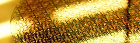
Our Electronic Materials Business
JSR is a global leader in cutting-edge materials for the semiconductor industry. We provide comprehensive solutions across the entire semiconductor manufacturing process and support customers to enhance yields and optimize productivity, thereby contributing to the advancement and mass production of next-generation devices.
Lithography Materials
The lithography process is a core technology that determines the scaling and performance of semiconductor devices. JSR offers a comprehensive portfolio that includes photoresists from i-line to EUV, as well as a variety of organic and inorganic multilayer materials.
Photoresists & Multilayer Materials
The lithography process is a core technology that determines the scaling and performance of semiconductor devices. JSR offers a comprehensive portfolio that includes photoresists from i-line to EUV, as well as a variety of organic and inorganic multilayer materials. By offering a comprehensive portfolio and advancing material designs that simultaneously enable high device performance and high reliability, we continuously support our customers’ process innovation fromcutting-edge nodes to legacy ones.
Process Materials
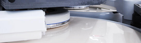
CMP processes, cleaning, and Wet SAM processes are essential steps in semiconductor manufacturing to achieve planarization and low defect levels in wiring and between layers. JSR provides the slurries and cleaning solutions required for these processes, achieving both high planarization performance and low defect levels.Slurries enable precise polishing control, while cleaning solutions effectively remove residual particles and metal impurities. Combining both products enables consistent process quality and high yields, thereby supporting the mass production of next-generation devices.
CMP Materials (Slurries/Cleaning Solutions)
CMP slurries and post-CMP cleaning solutions are essential to high-performance LSI manufacturing. JSR’s materials offer high planarization performance and selectivity, achieving defect reduction and high reproducibility to meet device scaling demands.
Cleaning Solutions
Functional cleaning solutions efficiently remove fine particles, metal ions, and reaction byproducts remaining on substrate surfaces before and after SAM treatment following etching.
Deposition Materials

JSR provides ALD /CVD precursors and dopants essential for forming the multilayer structures required in semiconductor manufacturing.
Our high-quality ALD precursors contribute to the mass production processes of complex 3D structures in advanced logic and memory semiconductors. We have a top-tier domestic supply capability for TEOS, a material widely used in CVD, and we also deliver high-quality products for compound and oxide semiconductor applications.
Precursors for ALD/CVD
Based on advanced molecular design, synthesis technology, and quality control systems, we enable atomic-layer-level film thickness control, achieving excellent film quality, uniformity, and step coverage. Our materials’ high purity, low metal contamination, and stable supply support a wide range of applications, including gate dielectrics, barrier metal, and wiring formation for advanced semiconductors.
Dopants
JSR provides high-purity dopant materials for controlling the electrical properties of semiconductor devices. We achieve high purity and precise concentration control, enabling uniform doping.
Advanced Electronic Materials
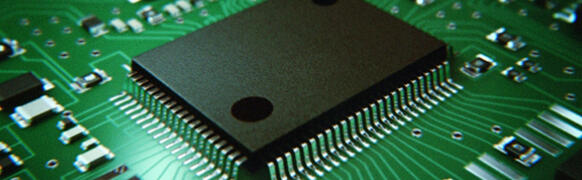
Leveraging polymer technologies cultivated over many years in the petrochemical business, JSR meets diverse high-quality market needs with materials such as dielectric materials used in semiconductor manufacturing and materials for high-density integration.
Thick Layer Plating Photoresists
JSR’s thick layer plating photoresists offer excellent resolution, resistance to various plating solutions, and robustness for vacuum processes, and can be used for flip-chip bump formation, micro-bump formation, and redistribution layer (RDL) formation of semiconductor packages. With a single spin-coating, the negative-tone resist achieves a film thickness of 100 µm.
Photo-Imageable Dielectric Materials
JSR’s materials are suitable for the redistribution layers and photo-imageable dielectrics used in WL-CSP (wafer-level chip-size packages) and SiP (system-in-package), as well as for organic passivation materials for semiconductor devices. We also offer PFAS-free products in response to growing societal concerns in recent years.
In addition, as a photo-imageable insulating film for redistribution layers targeted at packages that integrate resin and metal wiring, such as fan-out packages, we are developing a low-temperature-curable polyimide that can use alkaline developers, enabling lower process cost and reduced environmental impact.