FLOSFIA and JSR progress toward practical use of the world's first P-type semiconductor, Iridium Gallium Oxide -- Development of new iridium-based film formation materials for mass production creates a solution for realizing the ultimate SEMI ecology™ -
Tokyo and Kyoto, JAPAN – March, 15, 2023 - FLOSFIA Inc. (FLOSFIA) and JSR Corporation (JSR) announced today they have jointly developed a new iridium-based film deposition material as a solution for mass production of iridium gallium oxide (alpha-(IrGa)2O3)*1). This is the world’s first P-type power semiconductor*2 developed by FLOSFIA for use in combination with corundum-type gallium oxide (alpha-Ga2O3)*3. The use of this material allows for mass production in industrial applications as well as the expression of P-type characteristics, which is the most important characteristic of iridium gallium oxide.
In the industrial application of iridium gallium oxide, there were the following three problems in mass production:
① Iridium acetylacetonate (Ir(acac)3), a known source of iridium, is poorly soluble in water and has a slow crystal growth rate of less than 1/10 of that of gallium oxide, resulting in a lack of productivity.
② The coverage during crystal growth is poor, making it difficult to form a uniform film inside the trench.
③ Due to the poor filling efficiency inside the trench, a large amount of iridium-based film formation material is required for one film formation.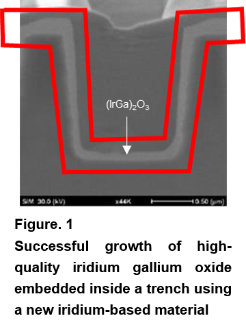 Given the iridium element has never been mass-produced as a semiconductor and the raw materials available are limited, it was necessary to develop a completely new iridium-based film forming material. The newly developed material achieves a high-speed crystal growth rate of more than 10 times higher than the conventional material, improves coverage inside trenches (see Fig.1), and reduces the use of iridium-based film deposition materials. As a result, the possibility of mass production application of iridium gallium oxide as a new P-type semiconductor in devices has dramatically increased, making significant progress toward the realization of FLOSFIA's goal of SEMI ecologyTM *4. Iridium gallium oxide used in combination with gallium oxide was successfully demonstrated in a JBS structure *5. Iridium gallium oxide is an ultra-wide bandgap semiconductor *6 with an extremely large bandgap of approximately 5 eV and a high hole concentration of 1 x 1019 cm-3, expecting its applicability to a wide-range of device designs assuming high-electric fields. This provides a solution for mass producibility by enabling early application to a wide range of power converters, including inverters used in the frequency range below 100 kHz.
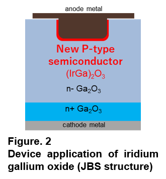
The results of our study are as follows:
We aimed to apply iridium gallium oxide to a JBS structure that is supposed to be embedded in a trench structure (Fig.2). After fabricating a trench structure in part of the gallium oxide n- layer, we embedded the iridium gallium oxide. At this time, we used FLOSFIA's proprietary MIST DRYTM method*7 for crystal growth but used a new iridium-based film formation material that we jointly developed as an iridium source in the solution. By using this new material, we confirmed the growth rate is more than 10 times higher than the conventional one. Cross-sectional observation of this trench structure by SEM confirmed the film thickness distribution of iridium gallium oxide was uniform and the film was formed with good coverage (Fig.3).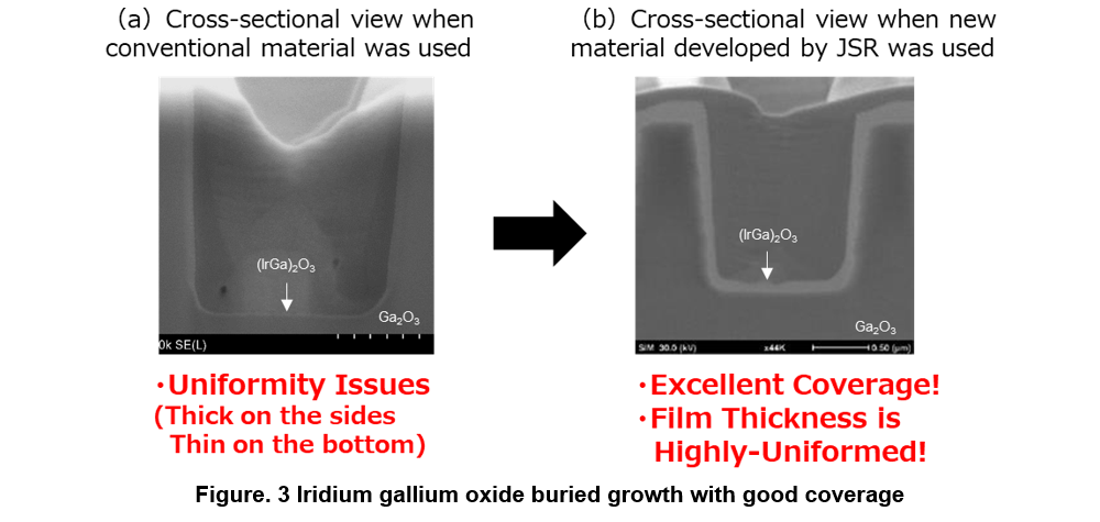
The JBS structure based on the results of this research will be applied from the second-generation diode of FLOSFIA's GaOTM series of corundum-type gallium oxide (alpha-Ga2O3) power devices. In addition to inverters and a wide range of other power converters used in the frequency range below 100 kHz, iridium gallium oxide will be applied to transistors such as MOSFET and IGBT. Examples of power converters include commercial power supplies such as AC adapters, robotic drive circuits, electric vehicles, white goods such as air conditioners and refrigerators, and solar cell power conditioners. The adoption of GaOTM power devices will challenge the limitations of miniaturization and cost reduction of the entire power converter *8. Depending on the type of equipment, for example, the degree of miniaturization of power converters can reach several 1/10, and the cost reduction is expected to reach 50% of the total power converters (estimated by FLOSFIA).
About FLOSFIA
FLOSFIA has named the reduction of three environmental impacts (Energy, Process, Material) caused by semiconductors SEMI ecologyTM and aims to promote a new power semiconductor, gallium oxide (Ga2O3), from Kyoto University.
・Company: FLOSFIA, INC.
・Address: 1- 29 Goryo-ohara, Nishikyo-ku, Kyoto
・President & CEO: Toshimi Hitora
・Capital: 4208.5 million yen (including capital reserve) (as of February 1, 2023)
・Establishment: March 31, 2011
・URL: https://www.flosfia.com
・Business Profile: Research, manufacture and sale of gallium oxide power devices
・Contact: E-mail info@flosfia.com
About JSR Corporation
JSR is promoting innovation to provide value to the world's leading-edge industries and exploring next-generation businesses that address social issues, while developing businesses globally with technological strengths centered on the digital solutions and life sciences businesses, including semiconductor materials. JSR and its CVC subsidiary JSR Active Innovation Fund LLC are equity participants in FLOSFIA.
・Company: JSR Corporation
・Address: Shiodome Sumitomo Building 22 F, 1-9-2 Higashishimbashi, Minato-ku, Tokyo
・Representative: Eric Johnson
・Capital: 23.37 billion yen (as of March 31, 2022)
・Establishment: December 10, 1957
・URL: https://www.jsr.co.jp/
・Business Profile: Research, manufacturing, sales, etc. in Digital Solutions Business, Life Sciences Business, Synthetic Resins Business
・Contact: E-mail jsr_koho@jsr.co.jp
Terminology
*1 Iridium gallium oxide (alpha-(IrGa) 2O3)
A ternary mixed crystal composed of gallium, iridium and oxygen with a corundum structure.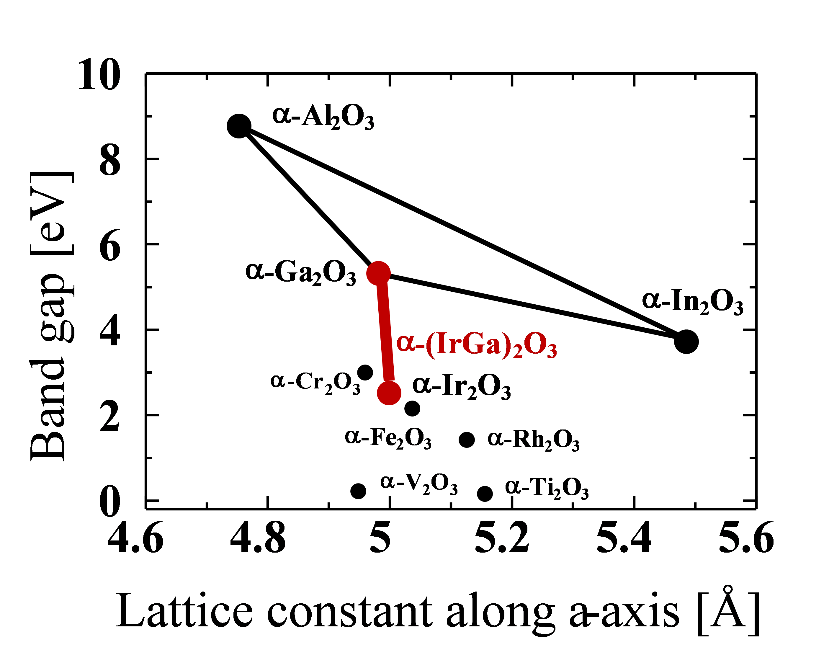
*2 "Power Semiconductors"
A semiconductor used for power conversion, it is used where a high voltage and a large current are applied compared to common semiconductors. It is used as a power device for transistors, diodes, and thyristors.
*3 "Gallium oxide (Ga2O3)"
This new material is attracting attention as a power semiconductor material. It is known to have various crystal structures, such as a beta-gallia structure (beta structure) in addition to a corundum structure (alpha structure). The beta-gallia structure is a unique crystal structure that takes only gallium oxide, while the corundum structure has various other family members, such as sapphire and indium oxide, in addition to gallium oxide, so it has been expected to grow crystals in heterostacking and to be used in devices.
*4 SEMI ecologyTM
The term SEMI ecology TM refers to the state in which the reduction of the impact on the global environment caused by the advancement of semiconductors has been maximized, and to the efforts being made to achieve this. We will contribute to the realization of a sustainable new future through the realization of a comprehensive ecology that includes "low energy loss," which reduces energy loss, "low process loss," which reduces manufacturing process loss, and "low material loss," which reduces the loss of finite global resources throughout peripheral circuits and systems. FLOSFIA collaborates with a variety of companies to achieve the ultimate in SEMI ecologyTM.
*5 JBS Structure
Junction Barrier Schottky Structure. The depletion layer spreading from the new embedded P-type semiconductor layer can mitigate the field strength at the Schottky interface and reduce the leakage current.
*6 Ultrawide Bandgap Semiconductor
SiC and GaN, which have a large bandgap of about 3 eV, are called wide bandgap semiconductors, while gallium oxide, diamond, and AlN, which have even larger bandgaps (generally more than 4 eV), are called ultlawide bandgap semiconductors.
*7 MIST DRY TM Method
FLOSFIA refers to a film formation method that FLOSFIA independently improved from the mist CVD method originally developed by a research group led by Professor Shizuo Fujita of Kyoto University. FLOSFIA synthesizes gallium oxide and controls its impurity concentration using the MIST DRYTM method.
*8 Limits to miniaturization and cost reduction of power converters
To reduce the size and cost of power converters, it is considered necessary to increase the operating frequency. If silicon (Si) is used, it is thought to be difficult to reduce the size of power converters because, for example, high frequency operation results in a large conversion loss requiring additional heat dissipation measures. In addition, if silicon carbide (SiC) is used as a new semiconductor material, high frequency operation is possible and power converters can be reduced in size, but its synthesis method and process technology are considered to have limitations in reducing the cost.