JSR introduces non-topcoat self-freezing ArF Photoresist for double patterning process
~ Responding to the diversification of semiconductor manufacturing processes ~
 02/22/2010
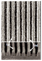
TOKYO - 22 February 2010 - JSR Corporation (President: Mitsunobu Koshiba) announced today that it has developed a non-topcoat self-freezing ArF photoresist for double patterning (a next-generation semiconductor manufacturing process used for 32nm half-pitch node and beyond), achieving 26nm half-pitch line and space patterns (refer to reference material 1). Since the introduction of JSR's self-freezing ArF photoresist (requiring a topcoat) in June last year, the newly-developed material is a result of continued efforts to respond to diversifying needs and to reduce the cost of processes in semiconductor manufacturing.
With the advancement of digital devices such as smartphones and audio players, as well as the technological advancements and improved power-saving features of personal computers capable of handling large content such as music, images and photos, the semiconductor industry will continue to pursue further pattern miniaturization .In order to respond to the technological advancements of our customers, JSR will further expand its semiconductor materials business, which is one of our core businesses.
Details of the new material will be announced at SPIE Advanced Lithography 2010, an international forum for lithography technologies in semiconductor manufacturing. Held in San Jose, California (USA), JSR will present on 24 February (US local time; presentation number: 7639-39).
The non-topcoat self-freezing ArF photoresist to be presented has a thermosetting function, whereby the material itself hardens during heat treatment, preventing it from dissolving when coated with the second exposure photoresist. In addition, JSR has proved that even without a topcoat, it is possible to keep defectivity (i.e. water marks, an issue in immersion exposure) to a minimum, as well as demonstrating that exposure is possible without damage to (by way of eluded material from the photoresists) the high-performing, delicate lens surface of the exposure tool. The material will further simplify the double patterning process for semiconductor manufacturing. Moreover, the material has improved resistance to high-speed scanning of exposure tools, which will offer increased productivity for our customers.
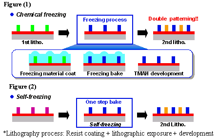
JSR offers many solutions to its customers depending on their chosen manufacturing processes and methods, such as combining freezing materials with leading-edge ArF photoresists, or combining self-freezing ArF photoresists with the TCX topcoat series (which have become an industry standard) for immersion exposure, and the newly-developed non-topcoat self-freezing ArF photoresist (refer to reference material 2).
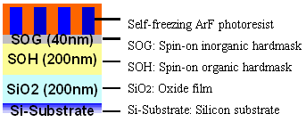
Additionally, in applying the company's own organic and inorganic spin-on hardmask materials to the aforementioned non-Topcoat self-freezing ArF photoresist, JSR has succeeded in microfabricating the silicon oxide substrate, just as it is done in the manufacturing of actual devices (refer to reference material 3).
JSR is comprehensively developing leading-edge semiconductor materials, supplying the global market with high quality and high-performing products, necessary in the manufacture of next-generation semiconductors. JSR's product lineup includes ArF photoresists, TCX topcoat series for immersion exposure, spin-on hardmask materials, high-density packaging materials and CMP materials.
<Reference materials>
1.Top-down and X-Sectional SEM image of 26nm half-pitch

2.Process comparison - chemical freezing versus self-freezing resist
3.Processing example when JSR's spin-on hardmask materials used
With the advancement of digital devices such as smartphones and audio players, as well as the technological advancements and improved power-saving features of personal computers capable of handling large content such as music, images and photos, the semiconductor industry will continue to pursue further pattern miniaturization .In order to respond to the technological advancements of our customers, JSR will further expand its semiconductor materials business, which is one of our core businesses.
Details of the new material will be announced at SPIE Advanced Lithography 2010, an international forum for lithography technologies in semiconductor manufacturing. Held in San Jose, California (USA), JSR will present on 24 February (US local time; presentation number: 7639-39).
The non-topcoat self-freezing ArF photoresist to be presented has a thermosetting function, whereby the material itself hardens during heat treatment, preventing it from dissolving when coated with the second exposure photoresist. In addition, JSR has proved that even without a topcoat, it is possible to keep defectivity (i.e. water marks, an issue in immersion exposure) to a minimum, as well as demonstrating that exposure is possible without damage to (by way of eluded material from the photoresists) the high-performing, delicate lens surface of the exposure tool. The material will further simplify the double patterning process for semiconductor manufacturing. Moreover, the material has improved resistance to high-speed scanning of exposure tools, which will offer increased productivity for our customers.
JSR offers many solutions to its customers depending on their chosen manufacturing processes and methods, such as combining freezing materials with leading-edge ArF photoresists, or combining self-freezing ArF photoresists with the TCX topcoat series (which have become an industry standard) for immersion exposure, and the newly-developed non-topcoat self-freezing ArF photoresist (refer to reference material 2).
Additionally, in applying the company's own organic and inorganic spin-on hardmask materials to the aforementioned non-Topcoat self-freezing ArF photoresist, JSR has succeeded in microfabricating the silicon oxide substrate, just as it is done in the manufacturing of actual devices (refer to reference material 3).
JSR is comprehensively developing leading-edge semiconductor materials, supplying the global market with high quality and high-performing products, necessary in the manufacture of next-generation semiconductors. JSR's product lineup includes ArF photoresists, TCX topcoat series for immersion exposure, spin-on hardmask materials, high-density packaging materials and CMP materials.
<Reference materials>
1.Top-down and X-Sectional SEM image of 26nm half-pitch

2.Process comparison - chemical freezing versus self-freezing resist
 | Figure (1) on the left shows the method when a freezing material is used and figure (2) shows the method when a self-freezing photoresist is used. Using the newly-developed non-topcoat self-freezing resist allows omission of the top coat application at the "1st litho. process" shown in figure (2). |
| As the pattern size shrinks, the photoresist material becomes thinner and as a result, directly etching the oxide becomes a difficulty. To overcome this, two hard mask (organic and inorganic) layers are coated between the photoresist and oxide film, allowing etching to occur from the upper to lower layers, eventually microfabricating the oxide film. |  |
 | |
| Data courtesy of: Hitachi High-Technologies Corporation | |


