


JSR and SEMATECH Succeed in Developing World's First Chemically Amplified EUV Resist Capable of 15-nm Resolution Patterns
- A Giant Step Toward EUV Lithography's Application in Commercial Production
 10/20/2011
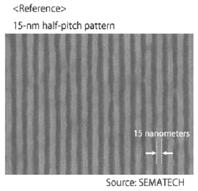
TOKYO - October 20, 2011- JSR Corporation (President: Nobu Koshiba), jointly with SEMATECH, a global consortium of chipmakers based in Texas, successfully demonstrated for the first time in the world that a 15-nm half-pitch*1 pattern can be formed with a chemically amplified photoresist using extreme ultraviolet (EUV) lithography. Practical application of EUV lithography has taken a great step forward with the realization of 10-nm level pattern formation.
*1: A 15 nm half-pitch means a pattern evenly spaced 15 nm apart.
EUV is said to have superior resolution because its exposure wavelength is 13.5 nanometers, less than a tenth of that of ArF (193 nanometers), which is commonly used in the most-advanced semiconductor manufacturing. While the chemically amplified photoresists that are the current standard are highly sensitive, the finest resolution of them, introduced by JSR in March 2011, stopped at 19-nm half-pitch. When exposed to light, the acid in chemically amplified photoresists diffuses and worsens resolution. JSR solved this issue by materially designing the photoresist to have a function that restricts the acid's diffusion behavior, among other functions, and so developed a chemically amplified photoresist for use with EUV capable of 15-nm half-pitch resolution.
SEMATECH presents a detailed explanation on October 19, 2011 at the 2011 International Symposium on Extreme Ultraviolet Lithography, an international EUV lithography technology conference held in Miami, Florida, USA.
While results of a 15-nm half-pitch pattern formation using a non-chemically amplified photoresist were presented at SPIE Advanced Lithography 2011, an international conference for the lithography field held this spring in the U.S.; the photoresist had less than half the photospeed of JSR's newly developed product, which poses an issue for its practical application.
Semiconductor products are spreading beyond computers into the communication, automobile, home electronics, and medical fields and are permeating people's daily lives. As such, reducing the size and enhancing the speed of semiconductor products is highly desirable to promote further development. The refinement of semiconductor circuits and the consequent refinement of patterning resolution is seen as the solution to this demand. Concentrating especially on photoresists, JSR pledges to meet the needs of the semiconductor industry by proactively developing the optimal group of products for use in EUV lithography.