History
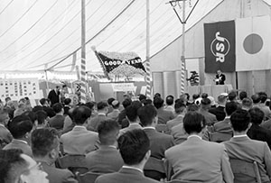
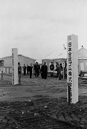
In 1957, Japan Synthetic Rubber Co., Ltd. Founded
1957
Company founded(as Japan Synthetic Rubber Co., Ltd.)in accordance with the Special Measures Law for the Synthetic Rubber Manufacturing industry.
1960s
Launching Synthetic Rubber Production in Japan
1960
Yokkaichi Plant began production and sales of butadiene,SBR,and SB latex lines.Osaka Branch was Opened.
1963
Sales of paper coating latex (PCL) began.
1964
JSR advanced into the field of synthetic resins and production of ABS resin began within the Yokkaichi Plant.
1968
The Chiba Plant was completed, and production of butadiene began.
1969
Changed company's status to private owned.
1970s
Began to Diversify the Business Portfolio while Surviving a Deep Slump
1971
The Kashima Plant was completed, and production of butadiene and SBR began.
1979
Sales of CIR (negative type photoresist) began. JSR advanced into the semiconductor materials business.
1980s
Creating New Businesses and Drive Diversification
1982
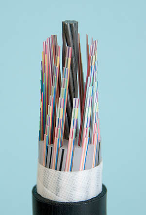
Importation and sales of optical fiber coating materials began.
1988
Sales of OPTMER AL (Alignment films for LCDs) and OPTMER SS (protective coatings for LCDs) began.
1989
Tsukuba Research Laboratory was officially opened.
1990s
Changing Corporate Name to JSR Corporation, Building a Global Production Structure
1993
UCB-JSR Electronics S.A. (Belgium) became wholly-owned subsidiary of JSR, and restarted by being renamed JSR ELECTRONICS N.V. Simultaneously JSR MICROELECTRONICS,INC. acquired U.S. operation as their subsidiary.
1996
A microphotoresist manufacturing subsidiary, JSR Electronics Kyushu Co., Ltd.(Saga) was established. Sales of epoxy type photo-curing resin having high accuracy, high-performance for photofabrication (stereolithography)
The ABS resin business was integrated with that of the Mitsubishi Chemical Corp., and a joint venture company, Techno Polymer Co., Ltd. was established.
1997
Construction work was completed for photoresist plant of JSR MICROELECTRONICS, INC.
Changed of corporate name to "JSR Corporation."
On 1997, we celebrated 40th anniversary of the founding of the company and changed our name to JSR Corporation. We had taken into consideration that our business portfolio had been expanding from synthetic rubbers and our target to expand further in the future. JSR's strategy to actively challenge to the new era, innovation and creativity had been reflected to the symbol design.
The blue square represents the universe; yellow arc represents the light before the rising sun. For JSR, the blue square means the excellence in our technology and sustainability of our company, and the yellow arc is our leading edge technology and activity. This represents our ambition to be an excellent company.
JSR will contribute to the world by technology and performance and would light the era by providing cutting edge technologies to the industry. This is what we would like to express from our symbol.
2000s
Expanding Fine Chemicals Business
2002
JSR Electronics Kyushu Co., Ltd., JSR Microelectronics, Inc. and JSR ELECTRONICS N.V. changed their names to "JSR Micro Kyushu Co., Ltd.," "JSR Micro,Inc." and "JSR Micro N.V." accordingly. Begins production of emulsion polymerization SBR consigned by Sumitomo Chemical Co., Ltd. Posts personnel dedicated to the electronic materials business in the Shanghai representative office to strengthen this business area in China.
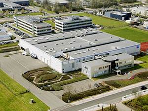
Completes new plant facilities for semiconductor materials in Belgium.
2003
Relocates the Head Office to HAMARIKYU Parkside Place, 6-10 Tsukiji5-chome, Chuo-ku, Tokyo, Japan.
2004
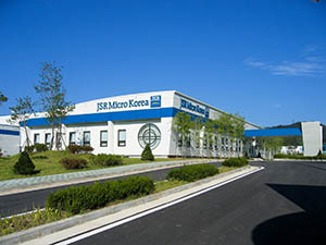
JSR Micro Korea Co., Ltd (plant for production of LCD Materials) was completed and started commercial production.
2006
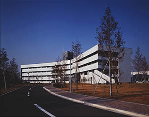
Completed the construction of new clean room facilities at the Yokkaichi research center.
Completed construction of precision machining pilot facilities at the Yokkaichi plant.
JSR Micro Taiwan Co., Ltd. (plant for production of LCD materials) was completed and started commercial production.
2007
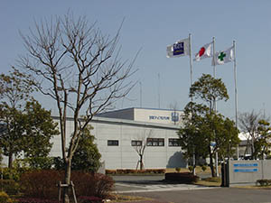
Completes Yokkaichi Training center
2008
JM Energy Completed construction of world's first commercial production plant of lithium ion capacitors.
2009
Joint-venture Techno Polymer Co., Ltd. becomes 100% subsidiary.
Relocates the Head office to Shiodome Sumitomo Bldg., 1-9-2 Higashi- Shimbashi, Minato-ku, Tokyo.
JSR Starts Operations at New Plant Facilities for Cutting-edge Lithography Materials in Response to Increase in Demand for ArF Photoresists
2010s
Expanding Life Sciences Business Aiming for Sustainable Growth
2011
Completed Increase of Manufacturing Capacity of Solution Polymerization Styrene-Butadiene Rubber (SSBR)
JM Energy Completed Construction of Manufacturing Plant, Evaluation Building and Safety Assessment Laboratory for Flat Prismatic Type Lithium Ion Capacitors
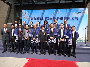
Established Diagnostic Products Joint Venture called "J&W Biotech Co., Ltd." in China
2012
Completion of J&W Beijing Biotech Co., Ltd Headquarters and Plant
2015
JSR jointly acquired KBI Biopharma, Inc., a contract developer and manufacturers of biopharmaceuticals in the United States
2018
Established Techno-UMG Co., Ltd. as an integrated ABS resin business.
Started operations of JSR Elastomer India Private Limited, a new subsidiary in India.
Completed aquisition of Crown Bioscience International.
2019
Established US Headquarters for JSR Life Sciences and North America Holding Company.
2020s
Building a Resilient Organization
2021
MEDICAL & BIOLOGICAL LABORATORIES CO., LTD. (MBL) becomes 100% subsidiary.
R&D Facility, JSR Bioscience and informatics R&D center (JSR BiRD) for New Business Incubations was opened.
EUV Pioneer Inpria Corporation becomes 100% subsidiary.
2022
Elastomers Business was transferred to ENEOS Corporation
2024
Tender offer by JICC-02, Ltd. for the Company's common stock, etc. was completed; JICC-02, Ltd. became the parent company and major shareholder of the Company.
Delisted from the Tokyo Stock Exchange Prime Market.
JSR merged with JICC-02; JICC-02 changed its name to JSR Corporation and took over its business.
2025
Medical and Biological Laboratories Co., Ltd. and JSR Life Sciences Corporation are transferred to Tokuyama Corporation.